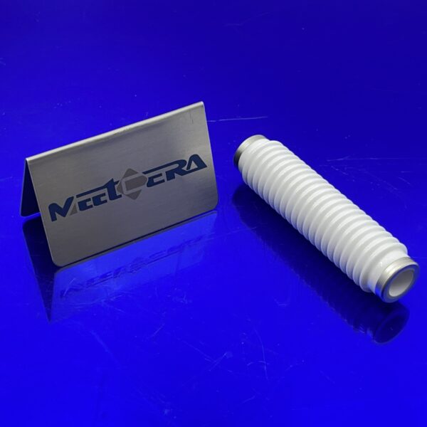
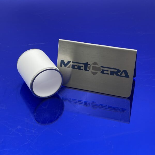
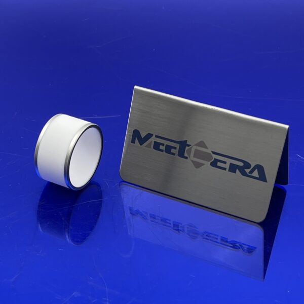
What Exactly Is Ceramic Metallization Technology?
When you look at many high-performance electronic components or industrial parts, you often see ceramic joined to metal. This connection is vital, but making it strong and sealed is not simple. Ceramic and metal are fundamentally different materials. This is where ceramic metallization technology1 comes in. It is a key process that makes these connections possible. People often ask me, "What is ceramic metallization?" I want to explain what this technology is and why it is so necessary for modern manufacturing.
Why do you need robust mechanical connections?
Components made from ceramic and metal often need to withstand physical forces – they need to be strong enough not to break under mechanical stress, vibration, or pressure.
This is a problem because without a strong bond connecting the ceramic to the metal, the joint will be the weakest point in the component. The natural forces trying to pull or push the ceramic and metal apart (including stresses from thermal expansion differences) will easily break a weak, non-metallized joint. This leads to structural failure of the component and potentially the entire system it is part of.
By creating a chemically and metallurgically bonded interface between the ceramic and the metal joining material, ceramic metallization technology enables the formation of high-strength joints. This strong bond allows mechanical loads to be transferred effectively between the ceramic and metal parts, ensuring the structural integrity of the final component.
What are the requirements for an airtight (leakproof) seal?
Many advanced applications require a perfect seal between ceramic and metal parts to prevent any leakage of gases or liquids.
This is a problem because achieving a truly hermetic seal2 requires a continuous, void-free bond line along the entire perimeter of the joint. As mentioned, without metallization, the braze alloy cannot wet the ceramic surface completely or consistently, leaving microscopic gaps at the interface. These tiny gaps, though invisible, act as leak paths that allow gases (like air or helium) or moisture to pass through, compromising vacuum integrity or allowing contaminants into sensitive areas.
Ceramic metallization technology is essential for creating hermetic seals because it allows the molten braze alloy to fully wet and flow across the designated joint area on the ceramic surface. This forms a continuous, dense, and void-free bond line between the ceramic and the metal joining material, effectively creating a perfect barrier against leaks.
In vacuum systems, for example, if the ceramic feedthrough seal is not hermetic, the vacuum is lost. Metallization is what makes that hermetic seal possible with ceramic.
How do I add electrical features to an insulator?
Ceramics like alumina are excellent electrical insulators, but many ceramic components, especially in electronics, need specific areas that can conduct electricity to serve as electrical pathways or connection pads.
This is a problem because you cannot just deposit metal onto a bare insulator surface and expect it to stick reliably or create defined, high-resolution conductive patterns needed for electronics. Standard printing or plating methods used for metals or polymers do not work effectively on bare ceramics for robust electrical features.
Ceramic metallization technology allows for the creation of precisely defined conductive metal patterns (traces, pads, vias) on the ceramic surface. These patterns transform areas of the insulating ceramic into functional electrical pathways or connection points, enabling the ceramic to serve as a substrate for mounting electronic chips and routing electrical signals.
What are the different methods of applying metallization?
There is no single "ceramic metallization" process. Different applications, ceramic types, and desired properties require different technological approaches.
This is a problem because relying on only one metallization method would limit the types of ceramic-to-metal joints or ceramic-based electronics you can create. A process optimized for high-temperature brazing of alumina might not work for soldering a different ceramic or creating very fine-line electronic traces. Choosing the wrong metallization technology for the specific need will result in poor performance or process failure.
Ceramic metallization technology is an umbrella term covering several distinct processes that achieve the goal of making ceramic surfaces bondable or conductive. These different technologies, like Moly-Manganese (Mo-Mn) or using Active Brazing Alloys (ABA)3, are selected based on factors such as the type of ceramic, the mating metal, the required joint strength, hermeticity level, and the intended processing temperature (e.g., brazing vs. soldering).
Types of Metallization Technologies
Two prominent examples illustrate different approaches within this field:
- Moly-Manganese (Mo-Mn) Metallization: This is a widely used thick-film process, particularly for alumina ceramics. A paste containing Molybdenum and Manganese powders (and sometimes glass frit) is printed onto the ceramic surface. The ceramic is then fired at very high temperatures (around 1500-1600°C) in a wet hydrogen atmosphere. This firing causes the Mo-Mn to bond to the ceramic, creating a slightly porous layer. This layer is then usually plated with Nickel to provide a surface that is easily wetted by standard braze alloys (like Copper-Silver eutectic).
- Active Brazing Alloys (ABA): This is a different approach where the metallization step is integrated into the brazing process itself. Active braze alloys contain a small amount of an "active" element, typically Titanium or Zirconium, mixed into the braze alloy (often a silver-copper alloy). When the ABA melts during brazing, the active element reacts directly with the ceramic surface, forming a thin reaction layer that allows the rest of the braze alloy to wet and bond to the ceramic without a separate metallization firing step beforehand.
| Technology | Process Overview | Bond Mechanism To Ceramic | Used For (Joining Method) | Typical Ceramics |
|---|---|---|---|---|
| Moly-Manganese | Paste print $\rightarrow$ High-temp firing $\rightarrow$ Plating | Reaction/Mechanical Interlocking | Brazing | Alumina |
| Active Brazing | Braze Alloy contains Reactive Element | Direct Chemical Reaction (in-situ) | Brazing | Alumina, AlN, Zirconia |
This table provides a simplified comparison of two key technologies.
Can Ceramic Metallization Achieve High-Precision Patterns?
Modern electronic chips have many connection points (pads) that are packed tightly around their edges or even across their surface.
This is a problem because the metallized pattern on the ceramic package or substrate must have corresponding pads that are just as small and precisely located as the chip’s pads. If the metallization process cannot create these small features accurately, it is impossible to reliably connect the chip to the package, for example, using wire bonding or flip-chip soldering. This leads to assembly failures, poor yields, and devices that do not work.
Yes, ceramic metallization technology must achieve high precision because it needs to create very small, accurately positioned conductive pads and features on the ceramic surface to match the miniaturized connection points on modern electronic chips.
I remember trying to connect a chip with 100-micrometer pitch pads onto a substrate made with older metallization technology. The pads on the substrate were not uniform, and wire bonding yield was terrible. We needed higher precision metallization.
Will the routing have multiple signals in a small area?
As electronic devices become more complex, they need to route many electrical signals and power lines between the chip and other parts of the circuit, often within a very small space on the package or substrate.
This is a problem because to route many signals in a small area, the conductive traces (lines) on the ceramic must be very narrow, and the space between them must also be very small. If the metallization process cannot create these fine lines and spaces with accuracy and consistency, signals might short together (bridging), or lines might break (opens). Also, for high-speed signals, precise line geometry is needed for signal integrity. Lack of precision limits the density of the circuit and the overall functionality you can put on the ceramic.
Ceramic metallization technology can create fine conductive lines and spaces on the ceramic surface, allowing for high-density routing of multiple electrical signals and power lines within the limited space of an electronic package or substrate.
Are there limitations to metallization methods?
Traditional or simpler ceramic metallization methods might not offer the high level of detail needed for the most advanced electronic designs.
This is a problem because methods like standard thick-film screen printing have inherent limitations on the minimum size of features they can reliably produce. The resolution is limited by the screen mesh size, paste particle size, and printing process control. If your design requires patterns finer than what standard methods can achieve, you cannot use those methods effectively. Trying to push them too far results in poor yield, inconsistent pattern quality, and unreliable electrical performance.
**While basic metallization techniques have resolution limits, the field of ceramic metallization technology includes advanced processes specifically developed to overcome these limitations and achieve muc
Isn’t ceramic quality important?
The surface properties of the ceramic substrate or package itself play a big role in how precise the metallization pattern can be.
This is a problem because a rough or uneven ceramic surface makes it very difficult to print or deposit fine metal patterns accurately and consistently. Jagged edges or inconsistencies in the ceramic surface topography transfer to the metallization pattern, reducing effective resolution and potentially causing electrical flaws like opens or shorts in fine lines. Without a smooth base, high-precision patterns are impossible.
Achieving high-precision metallization requires using high-quality ceramic substrates4 with very smooth, consistent surfaces. Ceramic manufacturers produce specialized polished or fine-grained ceramic materials specifically designed to serve as a high-quality base for fine-feature metallization.
Comparing Metallization Precision Levels
Different metallization technologies offer varying levels of achievable pattern precision. The choice depends on the requirements of the specific electronic design.
| Technology | Typical Line Width/Spacing (Micrometers) | Key Method(s) Used | Primary Benefit for Precision |
|---|---|---|---|
| Standard Thick Film | 100 and above | Screen Printing | Cost-effective |
| Advanced Thick Film | 50 – 100 | Improved Screen Printing | Balance of cost/performance |
| Thin Film | Below 50 (e.g., 10-25 or less) | Sputtering, Photolithography | Highest density/resolution |
This table gives a general idea of the different levels of precision you can expect from various metallization technologies.
What Pattern Precision Do You Need?
Your application requires conductive or bondable patterns on the ceramic with specific levels of detail, like very fine lines and spaces or very small, accurately placed pads.
This is a problem because different metallization technologies can achieve different levels of precision. If you choose a process that cannot produce the required minimum line width, space, or positional accuracy, the metallized pattern will not match your design. This prevents you from connecting to miniaturized chips, routing high-density circuits, or meeting critical electrical performance specifications, limiting your product’s functionality and size.
Evaluate the required pattern resolution, including minimum line width, minimum spacing, and tolerance on feature size and position. Applications needing very fine features (e.g., <50 µm lines) likely require thin-film metallization, while less demanding designs might use advanced thick-film (50-100 µm) or standard thick-film (>100 µm).
I had a client designing a high-frequency module. They initially thought thick film was fine, but their simulation showed line width variations would kill the signal integrity. Based on their need for precise 50 µm lines, I recommended advanced thick film.
How Much Mechanical Strength is Needed?
The ceramic-to-metal joint must reliably withstand specific mechanical forces during assembly and operation, such as tension, shear, vibration, shock, or constant load.
This is a problem because the mechanical strength of the final joint depends heavily on the quality of the bond created by the metallization and subsequent joining process (like brazing). If the chosen metallization method does not create a robust interface layer that promotes a strong bond between the ceramic and the mating metal part, the joint will be mechanically weak. It will be prone to failure under operational stresses, leading to component breakage and system downtime.
Assess the mechanical loads the joint will experience. Metallization processes that enable high-temperature brazing (like Moly-Manganese or Active Brazing Alloys) typically create very strong metallurgical bonds capable of withstanding demanding mechanical stresses and thermal cycling.
Is a Hermetic Seal Required?
Does your application need a joint that is perfectly sealed, preventing any passage of gases or liquids to maintain vacuum, protect sensitive components, or contain substances?
This is a problem because not all joining methods or metallization types result in a hermetic seal. If hermeticity is required and you choose a process that creates a porous metallization layer incompatible with hermetic brazing, or if the resulting joint contains microscopic leaks, the seal will fail. Contaminants will enter, or needed substances will escape, leading to performance degradation or failure in critical sealed environments (vacuum, medical, aerospace, harsh environments).
Determine if a hermetic seal is mandatory. If it is, you must choose a metallization process specifically designed to be compatible with hermetic brazing techniques5, such as Moly-Manganese (followed by plating) or Active Brazing Alloys, which create continuous, void-free interfaces.
For aerospace applications, where components must survive vacuum and extreme temperatures, hermeticity is non-negotiable. We always recommend metallization processes6 proven for hermetic brazing in these cases.
What are the Electrical Demands?
Does the metallized pattern need to carry significant electrical current, provide controlled impedance for high-frequency signals, or be compatible with specific chip bonding methods (like wire bonding or flip-chip)?
This is a problem because different metallization technologies offer different electrical properties. The thickness, composition, and geometry of the metal pattern affect its electrical resistance (current carrying capacity) and high-frequency characteristics. If the chosen process doesn’t meet these needs, the component might overheat, lose signal integrity, or be impossible to assemble correctly, leading to poor electrical performance or manufacturing failure.
Consider the electrical requirements. Thick-film metallization provides thicker layers for higher current. Thin-film offers precise geometry for impedance control and high-frequency signals. The top metal layer (plating) is chosen for compatibility with wire bonding (e.g., Gold) or soldering (e.g., Nickel/Gold).
What is the Operating Environment (Temperature, etc.)?
What is the temperature range the component will experience? Will it undergo repeated heating and cooling cycles? Will it be exposed to harsh chemicals, humidity, or radiation?
This is a problem because these environmental factors put stress on the metallization layer and the joint. Extreme temperatures can cause material degradation. Temperature cycling creates stress from CTE mismatch. Chemicals can cause corrosion. If the chosen metallization is not stable and durable in the specific operating environment, it can crack, delaminate, or corrode, leading to joint failure or loss of electrical function over time.
Evaluate the operational environment. Choose metallization materials and processes proven to be stable and reliable across the required temperature range, resistant to chemical exposure if needed, and capable of enabling joints that withstand thermal cycling stress.
Conclusion
In conclusion, ceramic metallization technology is the vital process of applying metal layers or patterns onto ceramic surfaces. Its purpose is to overcome the natural difficulty of bonding ceramics to metals and to enable the creation of electrical pathways on insulating ceramics. By modifying the ceramic surface to make it compatible with metal joining materials and processes like brazing, metallization allows for the manufacture of strong, reliable, and hermetic ceramic-to-metal joints and functional electronic substrates. Without this technology, many critical components and advanced devices used across electronics, aerospace, medical, and high-temperature industries would simply not be possible to produce with the required performance and reliability.
-
Explore this resource to understand the significance and applications of ceramic metallization technology in modern manufacturing. ↩
-
Learn about the critical role of hermetic seals in ensuring the integrity of vacuum systems and sensitive applications. ↩
-
Discover how Active Brazing Alloys enhance the bonding process in ceramic metallization, making it more efficient and effective. ↩
-
Explore this link to understand the significance of high-quality ceramic substrates in achieving precise metallization patterns. ↩
-
Discover the importance of hermetic brazing techniques in ensuring reliable seals in critical applications like aerospace and medical devices. ↩
-
Learn about various metallization processes and their applications to enhance your understanding of ceramic-to-metal bonding. ↩


No comment