What Exactly Are Ceramic Metallization Services?
Ceramic metallization services enable reliable bonding between ceramics and metals — critical for hermetic seals, electrical connections, and high-reliability assemblies in electronics, aerospace, medical, and power industries.
These specialized services apply conductive metal layers to ceramic substrates (alumina, AlN, zirconia, etc.) using techniques like Mo-Mn thick film, thin-film deposition, or active brazing alloys. Companies turn to expert providers when they lack the high-temperature furnaces, vacuum equipment, or process know-how required.Research Progress of Ceramic Metallization Technology
Meetcera offers a full range of ceramic metallization services — from base layer application to complete brazed assemblies — with strict quality control and fast turnaround.
1.Which Metallization Technologies Do We Support?
Different applications demand different processes. We provide multiple proven technologies so you get the optimal match for your ceramic material, joint strength, hermeticity, and cost targets.
- Mo-Mn / Tungsten Thick Film — high-strength brazing base for alumina (25–100 μm)
- Thin-Film Metallization — precision patterns for RF/microwave, sensors (0.1–5 μm, <15 μm resolution).Metallization of ceramics
- Active Metal Brazing (AMB) — direct bonding without prior metallization.Ceramic Brazing
- Hybrid & Custom Solutions — DBC, LTCC/HTCC multilayer, embedded metallization
2.Do We Apply Post-Metallization Plating?
Yes. The fired metallization layer often needs additional plating for solderability, wire bonding, or braze compatibility.
- Electroless / electrolytic Nickel (corrosion resistance, braze wetting)
- Gold (wire bonding, low contact resistance)
- Other options: Ni-P, Pd, Ag — directly over the base layer
One-stop plating avoids transfer risks and quality variation.
3.Service Portfolio Overview
| Tier | Key Processes | Layer Thickness / Resolution | Typical Applications | Key Performance Metrics |
|---|---|---|---|---|
| Base Metallization | Mo-Mn screen print + high-temp firing | 25–100 μm | HV insulators, RF windows | Adhesion >70 MPa, Thermal shock 500 cycles |
| Advanced Thin Film | Sputtering / E-beam evaporation | 0.1–5 μm, <15 μm lines | MEMS, quantum devices, microwave | Resistivity <5 μΩ·cm, Step coverage >95% |
| Active Brazing | ABA paste / vacuum brazing | — | Power modules, laser packages | Void <2%, Thermal cond. >200 W/m·K |
| Full Integration | Multilayer co-firing, brazed assembly | Up to 32+ layers | Space electronics, medical implants | Hermeticity <1×10⁻⁹ atm cc/s He |
4.Design & Engineering Support — Included
New to metallized ceramics? We help you:
- Select the right metallization process
- Optimize pad / pattern layout for manufacturability
- Design reliable ceramic-to-metal joints
- Avoid common failure modes (CTE mismatch, voids, stress cracks)
Early collaboration reduces iterations and speeds time-to-market.
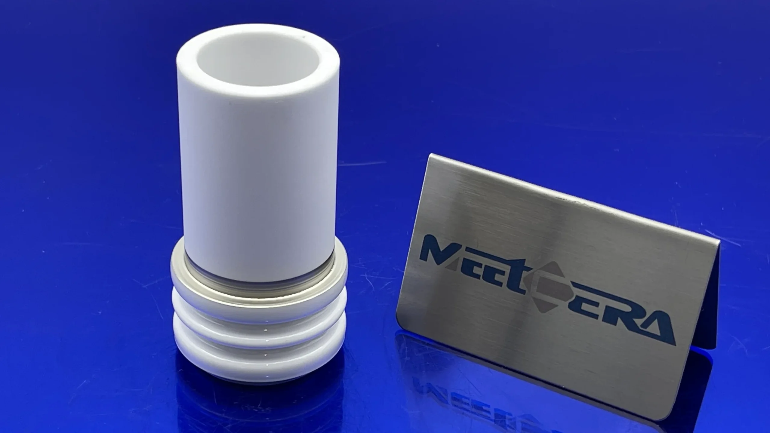
5.Integrated Brazing & Assembly Service
We don’t stop at metallization. Send us your metallized ceramics + mating metal parts — we perform controlled-atmosphere brazing and deliver finished hermetic assemblies.
Benefits: single-source accountability, reduced handling damage, faster debugging.
6.Full Quality Control & Testing
Every batch undergoes:
- Visual & dimensional inspection
- Adhesion / pull testing (ASTM F1147)
- X-ray / ultrasonic void detection
- Helium leak testing (<1×10⁻⁹ atm cc/s)
- Thermal cycling & shock (per MIL-STD or custom)
Full test reports provided.
7.Ready to Start Your Project?
Whether you need a quick prototype run, volume production, or help solving a difficult joining challenge, Meetcera’s ceramic metallization services deliver reliable, high-performance results.
→ Request a Quote →
→ View Metallized Ceramic Examples →
→ Free DFM feedback within 24 hours
We support small-batch R&D through high-volume manufacturing — with consistent quality and short lead times.