
Ceramic Metallization: 5 Critical Factors for High-Performance Electronic Design
Designing for harsh environments often comes down to a single question: how do you ensure a reliable, hermetic connection between ceramic and metal? Over my ten years in materials science, I’ve seen projects delayed simply because the ceramic metallization process wasn’t aligned with the application’s thermal or electrical requirements. Whether you are working on RF devices or power electronics, understanding these five core pillars will help you avoid costly prototype failures.
1. The Fundamentals of Ceramic Metallization Processes
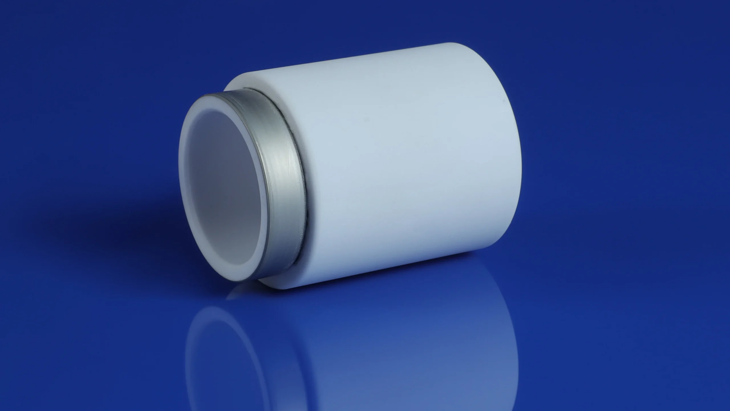
Ceramic metallization is an intricate, multifaceted process demanding precise control over numerous variables. To successfully create a functional and reliable bond, we must carefully consider each step, from material selection to surface preparation and process monitoring.
-
Deposition Method: The chosen method dictates the final metallization properties.
-
Thick Films: Sintering temperature profiles are vital for adhesion.
-
Thin Films: Vacuum levels and gas composition are critical for purity.
-
Electroplating: Precise current density control is required for uniformity.
-
Surface Preparation: A clean ceramic surface is the foundation of high-strength bonding. This involves cleaning to remove contaminants, followed by etching or roughening to provide mechanical interlocking.
-
Atmosphere Control: Maintaining a controlled environment is essential to prevent unwanted oxidation and chemical degradation during the bonding process.
2. Why Ceramic Metallization Matters in Modern Electronics
The diverse applications of ceramic metallization mirror the escalating performance requirements of modern electronics. It is the crucial enabler that allows ceramic substrates to interact with the broader electronic circuit.
- RF/Microwave Devices: In filters, low-noise amplifiers (LNAs), and power amplifiers (PAs), precise metallization patterns ensure signal integrity and fidelity.
- Power Electronics: Efficient heat management is non-negotiable. Our metallization solutions facilitate heat dissipation from semiconductors (MOSFETs, IGBTs) in electric vehicle inverters, motor drives, and renewable energy systems.
- LED Packaging: High-brightness LEDs require efficient heat extraction from the die, a task where properly metallized ceramics excel.
- Sensors: From automotive to medical implants, ceramic metallization provides the stable, long-term accuracy required for pressure, temperature, and gas sensing technologies.
3. Selecting the Optimal Metallization Technique
The selection of the optimal technique is linked to your specific performance requirements, cost constraints, and production volume. The following table provides a quick reference to help you determine which method best aligns with your engineering goals:
| Technique | Precision | Thermal Conductivity | Cost-Effectiveness | Best Application |
|---|---|---|---|---|
| Thick-Film | Moderate | Moderate | High | Consumer electronics |
| Thin-Film | Very High | Low/Moderate | Low | High-frequency RF devices |
| DBC | Moderate | Very High | Moderate | High-power modules [1] |
| AMB | High | Excellent | Low | Harsh environment/Power |
(Note: The selection should always be verified against industry standards for ceramic-to-metal bonding to ensure structural safety.)
4. Achieving Material Compatibility
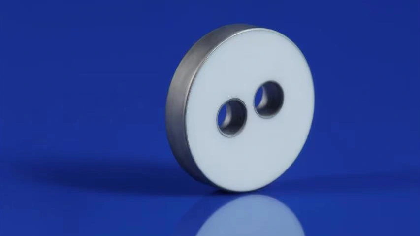
Achieving complete material compatibility in ceramic metallization demands a deep understanding of the interplay between the substrate and the metal layer.
- Substrate Choice: Alumina is cost-effective and versatile, while Aluminum Nitride (AlN) is preferred when higher thermal conductivity is needed.
- Thermal Expansion Matching: A mismatch in the Coefficient of Thermal Expansion (CTE) is the primary cause of fatigue failure. We must ensure the metal layer and the ceramic substrate expand and contract in harmony during temperature cycling.
- Interfacial Reactions: We carefully control interdiffusion to prevent the formation of brittle intermetallic compounds that could compromise the joint’s integrity.
5. Challenges and Limitations
Despite its widespread use, the technology faces constant evolution:
- High Processing Costs: Advanced techniques like Atomic Layer Deposition (ALD) require significant investment. Our role is to optimize the process to find the balance between performance and cost-effectiveness.
- Feature Size Resolution: As devices shrink, traditional thick-film printing faces resolution limits, driving the need for more advanced thin-film alternatives.
- Adhesion Reliability: Inadequate surface preparation remains a common failure point. We combat this through optimized interlayers (such as Chromium or Titanium) that act as adhesion promoters in materials science.
Expert Insights from Decades of Experience
From my ten years in this field, the biggest pitfall I’ve witnessed is choosing a metallization method without fully considering the long-term thermal cycling environment. Ceramic metallization is not just about adhesion; it’s about maintaining structural integrity under extreme stress. If you are currently in the design phase, I strongly recommend evaluating your CTE match early. It can save you months of development time and prevent premature system failure in the field.
*Need help selecting the right metallization strategy for your next project? Contact our engineering team today for a technical consultation.